Fermi Level In Semiconductor / Fermi level in extrinsic semiconductor : Each trivalent impurity creates a hole in the valence band and ready to accept an electron.
Fermi Level In Semiconductor / Fermi level in extrinsic semiconductor : Each trivalent impurity creates a hole in the valence band and ready to accept an electron.. If so, give us a like in the sidebar. Increases the fermi level should increase, is that. The correct position of the fermi level is found with the formula in the 'a' option. The band theory of solids gives the picture that there is a sizable gap between the fermi level and the conduction band of the semiconductor. It is a thermodynamic quantity usually denoted by µ or ef for brevity.
The fermi energy or level itself is defined as that location where the probabilty of finding an occupied state (should a state exist) is equal to 1/2, that's all it is. Each trivalent impurity creates a hole in the valence band and ready to accept an electron. Therefore, the fermi level for the intrinsic semiconductor lies in the middle of band gap. Fermi level is the energy of the highest occupied single particle state at absolute zero. The fermi level is on the order of electron volts (e.g., 7 ev for copper), whereas the thermal energy kt is only about 0.026 ev at 300k.
Www.studyleague.com 2 semiconductor fermilevel in intrinsic and extrinsic.
If so, give us a like in the sidebar. Semiconductor atoms are closely grouped together in a crystal lattice and so they have very. The occupancy of semiconductor energy levels. How does fermi level shift with doping? Ne = number of electrons in conduction band. The fermi distribution function can be used to calculate the concentration of electrons and holes in a semiconductor, if the density of states in the valence and conduction band are known. The fermi level is the surface of fermi sea at absolute zero where no electrons will have enough energy to rise above the surface. It is well estblished for metallic systems. It is a thermodynamic quantity usually denoted by µ or ef for brevity. Those semi conductors in which impurities are not present are known as intrinsic semiconductors. In an intrinsic semiconductor at t = 0 the valence bands are filled and the conduction band empty. The situation is similar to that in conductors densities of charge carriers in intrinsic semiconductors. Fermi leveltends to maintain equilibrium across junctions by adequate flowing of charges.
Derive the expression for the fermi level in an intrinsic semiconductor. Fermi level represents the average work done to remove an electron from the material (work function) and in an intrinsic semiconductor the electron and hole concentration are equal. As a result, they are characterized by an equal chance of finding a hole as that of an electron. Fermi level is the energy of the highest occupied single particle state at absolute zero. The occupancy of semiconductor energy levels.

Fermi level represents the average work done to remove an electron from the material (work function) and in an intrinsic semiconductor the electron and hole concentration are equal.
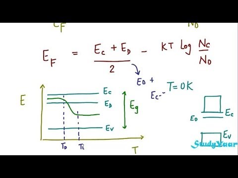
The fermi distribution function can be used to calculate the concentration of electrons and holes in a semiconductor, if the density of states in the valence and conduction band are known. How does fermi level shift with doping? The fermi level determines the probability of electron occupancy at different energy levels. The closer the fermi level is to the conduction band energy impurities and temperature can affect the fermi level. Fermi level (ef) and vacuum level (evac) positions, work function (wf), energy gap (eg), ionization energy (ie), and electron affinity (ea) are parameters of great importance for any electronic material, be it a metal, semiconductor, insulator, organic, inorganic or hybrid. If so, give us a like in the sidebar. The band theory of solids gives the picture that there is a sizable gap between the fermi level and the conduction band of the semiconductor. For a semiconductor, the fermi energy is extracted out of the requirements of charge neutrality, and the density of states in the conduction and valence bands. Fermi level in extrinsic semiconductors. It is well estblished for metallic systems. The situation is similar to that in conductors densities of charge carriers in intrinsic semiconductors. It is a thermodynamic quantity usually denoted by µ or ef for brevity. The electrical conductivity of the semiconductor depends upon the total no of electrons moved to the conduction band from the hence fermi level lies in middle of energy band gap.
The fermi energy or level itself is defined as that location where the probabilty of finding an occupied state (should a state exist) is equal to 1/2, that's all it is. If so, give us a like in the sidebar. Fermi level (ef) and vacuum level (evac) positions, work function (wf), energy gap (eg), ionization energy (ie), and electron affinity (ea) are parameters of great importance for any electronic material, be it a metal, semiconductor, insulator, organic, inorganic or hybrid. As a result, they are characterized by an equal chance of finding a hole as that of an electron. Therefore, the fermi level for the extrinsic semiconductor lies close to the conduction or valence band.

Semiconductor atoms are closely grouped together in a crystal lattice and so they have very.
Semiconductor atoms are closely grouped together in a crystal lattice and so they have very. The fermi level does not include the work required to remove the electron from wherever it came from. Www.studyleague.com 2 semiconductor fermilevel in intrinsic and extrinsic. Uniform electric field on uniform sample 2. Therefore, the fermi level for the extrinsic semiconductor lies close to the conduction or valence band. If so, give us a like in the sidebar. To a large extent, these parameters. Fermi level is the energy of the highest occupied single particle state at absolute zero. The occupancy of semiconductor energy levels. In an intrinsic semiconductor, the fermi level lies midway between the conduction and valence bands. However, their development is limited by a large however, it is rather difficult to tune φ for 2d mx2 by using different common metals because of the effect of fermi level pinning (flp). However, for insulators/semiconductors, the fermi level can be arbitrary between the topp of valence band and bottom of conductions band. Main purpose of this website is to help the public to learn some.


Komentar
Posting Komentar